| T O P I C R E V I E W |
| Anubha |
Posted - Nov 15 2017 : 07:51:13
Hi
I was trying to build a model which has two sensors placed on top of each other. Here are my code files and text files in fastcap2:
**code file**
* Plate 1 lower contact
C capacitor_contact_sides.txt 0.01 0.0 0.0 0.00
C plate.txt 0.01 0.0 0.0 0.00+
C plate.txt 0.03 0.0 0.0 0.02+
* dielectric medium
D capacitor_diel_sides.txt 0.01 0.03 0.0 0.0 0.02 0.05 0.05 0.05 -
* Plate 1 upper contact
C capacitor_contact_sides.txt 0.03 0.0 0.0 0.08+
C plate.txt 0.03 0.0 0.0 0.08 +
C plate.txt 0.03 0.0 0.0 0.1+
* Plate 2 lower contact
C capacitor_contact_sides.txt 0.05 0.0 0.0 0.1+
C plate.txt 0.05 0.0 0.0 0.12+
* dielectric medium
D capacitor_diel_sides.txt 0.01 0.05 0.0 0.0 0.12 0.15 0.15 0.15 -
* Plate 2 upper contact
C capacitor_contact_sides.txt 0.01 0.0 0.0 0.18+
C plate.txt 0.05 0.0 0.0 0.18 +
C plate.txt 0.01 0.0 0.0 0.2
**txt file- capacitor_contact_sides.txt**
Q c 5 5 0 5 0 0 5 0 0.02 5 5 0.02
Q c 0 5 0 5 5 0 5 5 0.02 0 5 0.02
Q c 5 0 0 0 0 0 0 0 0.02 5 0 0.02
Q c 0 0 0 0 5 0 0 5 0.02 0 0 0.02
End
**txt file- capacitor_contact_sides.txt**
Q d 5 5 0 5 0 0 5 0 0.06 5 5 0.06
Q d 0 5 0 5 5 0 5 5 0.06 0 5 0.06
Q d 5 0 0 0 0 0 0 0 0.06 5 0 0.06
Q d 0 0 0 0 5 0 0 5 0.06 0 0 0.06
End
**txt file-plate.txt**
Q p 0 0 0 5 0 0 5 5 0 0 5 0
End
My questions are:
1. I am trying to compute the capacitances between 2 cuboid dielectric films placed on top of each other, each of which have Lenght (in X plane)= 5cm, Breadth (in Y plane) = 5cm and depth (in Z-plane of each film= 1mm). Is this the correct code to compute the capacitance matrix?
2. My second question is regarding the dimensions. In one of the forums, you mentioned that the software doesn't compute the results if the dimensions are below its threshold, therefore, as per your suggestion, I have multiplied all the coordinates by 100 (so the X,Y,Z coordinates of each dielectric film are now 5, 5, 0.1) and have divided the permittivities by 100 (actual permittivity of 2 films were 3 and 5, now in the code they are 0.03 and 0.05, also the permittivity of free space is now 0.01). Is this the correct way to normalize the dimensions?
PS: The thickness of the dielectric medium comprises of thickness of upper and lower capacitor contact sides(0.04) and thickness of the dielectric medium (0.06)
3. Does the capacitance matrix take into account the mutual and fringe capacitance, so I reckon that the capacitance evaluation formula used by the software isn't very straight forward like Capacitance = (Area*relative permittivity * air's permittivity)/distance
I apologize if my question is "stupid". I am asking this because when I tried calculating the capacitance matrix of a singular cuboid film, and my capacitance matrix in faster cap had a different result than the numerical formula.
4. My last question is that when I am running the code, I am getting errors like-" Capacitance matrix is not diagonally dominant due to row 1"
What does it mean? and whats wrong in my code? Also I have to increase the relative tolerance to 0.1 (from 0.01) to run the code.
Thanks a lot in advance
Anubha
Anubha |
| 9 L A T E S T R E P L I E S (Newest First) |
| Enrico |
Posted - Nov 25 2017 : 11:54:31
Hi Anubha,
I think you copied the same link twice. Never mind, I believe the second file is just a triangle definition. I copy here the files as I reconstructed them:
- triangle.lst:
* Three plates structure
*
* lower contact
*
* triangle.txt : geometry file name
* 2.0 : permittivity
* 0.0 0.0 0.0 : 3D offset
C triangle.txt 2.0 0.0 0.0 0.0
* dielectric interface
*
* triangle.txt : geometry file name
* 2.0 : outer permittivity
* 1.0: inner permittivity
* 0.0 0.0 0.25 : 3D offset
* 0.25 0.25 0.0 : outer reference point
D triangle.txt 2.0 1.0  0.0 0.0 0.25  0.25 0.25 0.0

* upper contact
*
C triangle.txt 1.0 0.0 0.0 1.0
- triangle.txt:
0 unit triangle

T triangle 0 0 0  1 0 0  0 1 0
Now, you defined two conductor triangles embedded in two different mediums with a dielectric interface in between. However, the model is too crude here.
FasterCap can automatically refine the geometry, but cannot define the geometry in your stead. Actually, the dielectric interface you defined is just another triange, this means that from an electromagnetic point of view, you are defining boundary conditions between the two mediums only within that restricted area. And what about the field at the sides? There are no conditions there, since you did not complete the definition of a dielectric volume. This unbalances the potential matrix, resulting in a non-symmetrical capacitance matrix.
g1_triangle  5.34287e-011 -6.3693e-012
g2_triangle  -1.02166e-011 2.62006e-011
Now you have two options. Either you define a dielectric interface that is much larger than the two triangles, so you 'intercept' almost all the field lines, or you improve the definition of your dielectric interface, e.g. adding sides. I improved the definition using the latter approach:
* Three plates structure
*
* lower contact
*
* triangle.txt : geometry file name
* 2.0 : permittivity
* 0.0 0.0 0.0 : 3D offset
C triangle.txt 2.0 0.0 0.0 0.0
* dielectric interface
*
* triangle.txt : geometry file name
* 2.0 : outer permittivity
* 1.0: inner permittivity
* 0.0 0.0 0.25 : 3D offset
* 0.25 0.25 0.0 : outer reference point
D triangle.txt 2.0 1.0  0.0 0.0 0.25  0.25 0.25 0.0
D sides.txt 2.0 1.0  0.0 0.0 0.0  0.25 0.25 0.0

* upper contact
*
C triangle.txt 1.0 0.0 0.0 1.0
- sides.txt:
0 unit triangle sides

Q sides 0 0 0  1 0 0  1 0 0.25  0 0 0.25
Q sides 1 0 0  0 1 0  0 1 0.25  1 0 0.25
Q sides 0 1 0  0 0 0  0 0 0.25  0 1 0.25
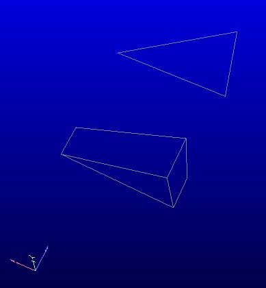
Now if you run the simulation, you get:
g1_triangle  4.61477e-011 -7.13998e-012
g2_triangle  -9.09469e-012 2.63849e-011
that, as you can see, is much improved in terms of symmetry. To further improve the symmetry, you'll probably need to improve the geometry again. You have the lower plate that is embedded in a dielectric medium of relative permittivity 2.0, but the dielectric medium covers only the top of the panel; its bottom side is still defined as in contact with the same medium, while in fact it should be in the second medium with relative permittivity 1.0. So you should give a thickness to this panel, making it a slab, and properly define the relative permittivity of the medium in contact with every side.
You may, in alternative, make the dielectric medium volume large and completely embed your panel. This is up to you and depends on the geometry you need to simulate.
Again, I suggest you to study the sample input files, available in the Samples directory, in particular:
- capacitor_simple_diel.lst:
* Simple parallel plate capacitor with inhomogeneous dielectric
*
*
* This capacitor is made by two square metal contacts
* filled with an inhomogeneous dielectric medium
*
* If fringing fields are neglected, the capacitance as per analytical formula
* is the series of two capacitors: the first capacitor has capacitance
* C1 = e0*er1*S/ (d/2), the second C2 = e0*er2*S/ (d/2), where S is
* the surface of the armors and d is their distance.
* In this case S = 1, d = 0.01, er1 = 1, er2 = 2; therefore
* C1 = 8.854e-12 * 1 * 1 / 0.0005 = 1.77e-8
* C2 = 8.854e-12 * 2 * 1 / 0.0005 = 3.54e-8
* therefore C = C1 // C2 = 1.18e-8
*
* Remark: given the high geometrical ratio 1:1000 between the plate side and
* the plate distance, for proper solution convergence you need to set FasterCap's
* '-d' parameter to 0.1 or lower values.
*
*

* lower contact
C plate.txt  1.0  0.0 0.0 0.0

* dielectric interface
D plate.txt 2.0 1.0  0.0 0.0 0.0005  0.0 0.0 0.001

* upper contact
C plate.txt  2.0  0.0 0.0 0.001
- capacitor.lst:
* Capacitor
*
* This capacitor is made by a dielectric material with relative permittivity
* equal to 3.0, sandwiched between two square metal contacts
* with finite thickness

* lower contact
C capacitor_contact_sides.txt  1.0  0.0 0.0 0.0 + 0xd8d8d8ff
C plate.txt  1.0  0.0 0.0 0.0 + 0xd8d8d8ff
C plate.txt  3.0  0.0 0.0 0.2  0xd8d8d8ff

* dielectric medium
D capacitor_diel_sides.txt  1.0  3.0  0.0 0.0 0.2  0.5 0.5 0.5 - 0xa793b4ff

* upper contact
C capacitor_contact_sides.txt  1.0  0.0 0.0 0.8 + 0xd8d8d8ff
C plate.txt  3.0  0.0 0.0 0.8 + 0xd8d8d8ff
C plate.txt  1.0  0.0 0.0 1.0  0xd8d8d8ff
As a final remark, please note that you may still have, in general, some small residual asymmetry in the capacitance matrix. This may be due to numerical errors, and the best way to approximate the real value is to average it. FastCap2 does this automatically, and therefore always gives you a symmetric matrix (with the notable exception of the case when you remove a column from the solution, see FastCap2 manual; in this case of course FastCap2, missing one or more columns in the solution, cannot average). FasterCap exposes you to the calculated matrix as it is, so you can realize if there are issues with your input geometry, as in this case.
Best Regards,
Enrico
|
| Anubha |
Posted - Nov 20 2017 : 06:21:32
quote:
Originally posted by Anubha
Hi Enrico,
I saw an example on treatment of dielectrics in faster cap.Here is the link:
ht*ps://w*w.fastfieldsolvers.com/Papers/The_Treatment_of_Dielectrics_in_FasterCap_WP130527_R01.pdf
On page 6 and 7 of this pdf, you have illustrated an example of a simple 3 panel structure.
Now, on running the code files in faster cap
(Here are the links:
ht*ps://drive.google.com/open?id=1hWDNhPmsDm6xMFuWGTEJMvGNALiZcjv3
and
ht*ps://drive.google.com/open?id=1hWDNhPmsDm6xMFuWGTEJMvGNALiZcjv3)
, I found that the diagonal capacitance of the Maxwell capacitance matrix is unsymmetrical/different.
I think the mutual capacitance between two conductors should be the same.
That is, C12=C21
(See page 3 on another example file:
ht*ps://w*w.fastfieldsolvers.com/Papers/The_Maxwell_Capacitance_Matrix_WP110301_R01.pdf)
Can you please explain why does the capacitance matrix doesn't have symmetrical values of C12 and C21 in this case?
Thanks
Anubha
Anubha |
| Anubha |
Posted - Nov 20 2017 : 06:20:06
Hi Enrico,
I saw an example on treatment of dielectrics in faster cap.Here is the link:
ht*ps://w*w.fastfieldsolvers.com/Papers/The_Treatment_of_Dielectrics_in_FasterCap_WP130527_R01.pdf
On page 6 and 7 of this pdf, you have illustrated an example of a simple 3 panel structure.
Now, on running the code files in faster cap
(Here are the links:
ht*ps://drive.google.com/open?id=1hWDNhPmsDm6xMFuWGTEJMvGNALiZcjv3
and
ht*ps://drive.google.com/open?id=1hWDNhPmsDm6xMFuWGTEJMvGNALiZcjv3)
, I found that the diagonal capacitance of the Maxwell capacitance matrix is unsymmetrical/different.
I think the mutual capacitance between two conductors should be the same.
That is, C12=C21
(See page 3 on another example file:
ht*ps://w*w.fastfieldsolvers.com/Papers/The_Maxwell_Capacitance_Matrix_WP110301_R01.pdf)
Can you please explain why does the capacitance matrix doesn't have symmetrical values of C12 and C21 in this case?
Thanks
Anubha |
| Anubha |
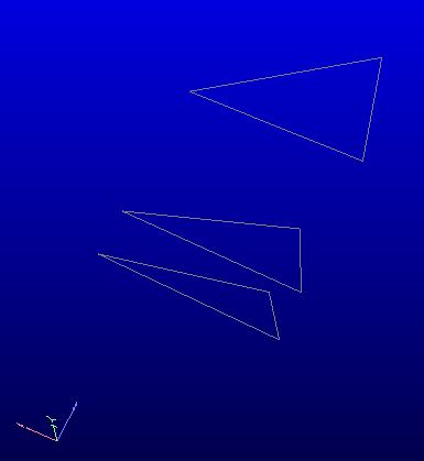
Posted - Nov 20 2017 : 05:30:50
Here are my code files for the above image. Please tell me whats wrong in the code :)
ht*ps://drive.google.com/open?id=1FYwWeNVh45wESfHOwrO_n987S9F-tvqz
Thanks
Anubha
Anubha |
| Anubha |
Posted - Nov 20 2017 : 05:27:07
ht*ps://drive.google.com/open?id=1O36RcwXvNs_lMQDE-ZxaQzN-6-9c6bE5
Anubha |
| Anubha |
Posted - Nov 20 2017 : 05:21:20

Anubha |
| Enrico |
Posted - Nov 17 2017 : 14:21:53
Actually your input file is faulty. And of course it is not normal for FasterCap to run for such a long time for a simple model like this one.
I strongly suggest to start with the sample files, reading the online embedded help in FasterCap, as well as FastCap2 manual. Once you have a grasp on how the simulator works, you can try more complex models.
Regarding however your problem at hand, actually I don't fully understand what you are trying to achieve. What do you mean by 'the capacitance of a dielectric medium'? Seems to me you want to know the capacitance of a parallel plate capacitor when there is a dielectric sheet in between, so using the parallel plate capacitor as a sensor. Then you have a second dielectric sheet, and I am not sure how you combine the metallic plates. If you can provide a simple drawing, I may be able to provide you better advice.
Best Regards,
Enrico
|
| Anubha |
Posted - Nov 16 2017 : 07:44:43
Hi Enrico,
Thanks for your reply.
I am using fastercap, not fast cap and the software is taking ages to compute the results. Does it normally take a day or so to get the results? Or is it because of the dimensions I have chosen (mie is a thin film with thickness 1mm)?
Is this the right code to run in fastercap?
Do we always need to take "capacitor contact sides" (in the code)
to analyse the capacitance matrix of a dielectric medium. Also how does the depth of conductive contact sides affect the results? For example, the overall depth of the cuboid here is 1mm, wherein the depth of the dielectric medium is 0.6 mm and that of the contact plates is 0.4mm. How will it affect my results if I change their depths?
I just want to build a simple model where two dielectric plates are overlapped and are on top of each other. Please help me write a code for this model. Also, I am getting a capacitance matrix of dimensions 2 by 2 using this code. Can you tell me how that matrix is distributed?
Anubha |
| Enrico |
Posted - Nov 15 2017 : 22:44:29
Dear Anubha,
let me answer your questions in a different order.
Point 3:
FastCap2, as well as FasterCap, does not use analytical formulae, but calculates the capacitance by solving the Maxwell equations in the electrostatic case (so actually it solves the Poisson's equation). Therefore, to the limit of the numerical errors, as well as of the method used, the solution is accurate and does include all field contributions (this is the so called 'field solver accuracy'). Full details about the formulation of the problem, as well as the algorithms used for the solution are available from the "Publications" page under the menu "Literature" of our web site. This is the difference between our open source solvers and other third party software, that use close-box algorithms and code that you cannot access, and therefore fully understand.
Point 1:
Are you using FastCap2 or FasterCap? If you are using FastCap2 this is not the right code, as FastCap2 is not able to automatically refine the geometry, and the input model is too crude
Point 2:
Actually you do not need to scale the model for such modest requirements in numerical precision. You may have issues in simulating structures in the nanometer range. In any case my suggestion is not to scale the permittivity, but to scale the result. To be clear, if for a structure of 1 mm you simulate instead a scaled-up structure of 1 meter and get 1 Farad as a result, this means that the original 1 mm structure has a capacitance of 1 milliFarad.
I'm not sure instead about your comment about the dielectric. I may recommend however to visualize your input file in FastModel, and remember that no panel is allowed to overlap, even partially, any other panel.
Point 4:
This is usually the result of a poor discretization or a flag of overlapping panels. In some case of high dimensional ratios in one of the dimension with respect to the others (e.g. a very flat contact) you need, in FasterCap, to play with the parameters, see the samples files installed with FasterCap (if you are using FasterCap)
Best Regards,
Enrico
|
|
|